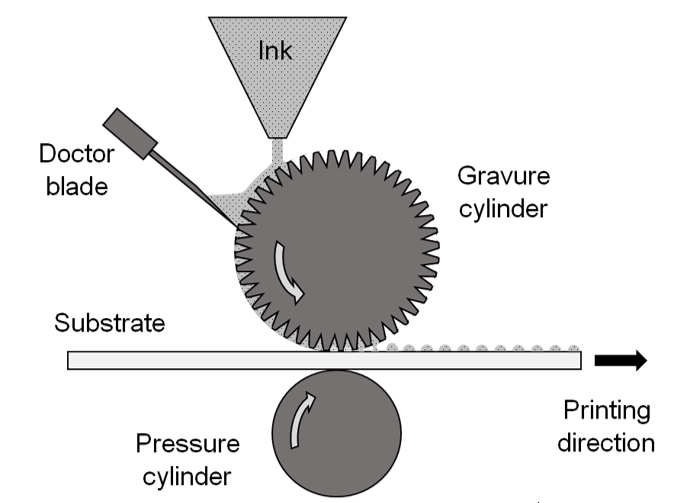
Piezo-semiconducting zinc oxide (ZnO) nanowires (NWs) are excellent candidates for the fabrication of energy harvesters, mechanical sensors, piezotronic and piezophototronic devices [1]. They are grown typically from thin seed layers. Low temperature fabrication methods are required for their integration on flexible substrates. Vacuum-free methods of deposition will eventually reduce their fabrication cost. In PULSE-COM, within a strong collaboration of ENEA and UGA partners [2], gravure printing method has been used to deposit thin layers of ZnO on flexible substrates. Gravure printing is one step method to directly deposit low viscosity inks over large area substrates, it is low cost and compatible with low temperature (See Fig 1.) [3]. Good quality ZnO NWs have been grown from these seed layers via Chemical Bath deposition at low temperature [4]. The grown NWs present small diameters, good alignment and density (See Fig 2.). The electromechanical quality of the grown NWs has been evaluated via Piezoresponse Force Microscopy (PFM). This technique gives us access to the amplitude and phase of the NWs piezo-induced deformation when an AC electric field is applied on them using an AFM tip (See Fig 3.). PFM measurements show that the grown NWs have homogeneous polarity and similar piezo-response comparable with other conventional techniques (i.e. Atomic Layer Deposition, requiring vaccum and high temperatures) (See Fig 4.). This work paves the way to the fabrication of flexible piezoelectric devices.

Fig 1. Gravure printing method.

Fig 2. SEM images of the ZnO NW grown on as-printed (not sintered) ZnO seed layer on ITO/PET flexible substrate.

Fig 3. (a )PFM principle. PFM images of (b) topography, (c) amplitude, and (d) phase of the ZnO NWs grown on as-printed (not sintered) ZnO seed layer/ITO/PET substrates.

Fig 4. Piezoelectric amplitude and phase histograms of ZnO NWs grown on as-printed (not sintered) ZnO seed layer/ITO/PET substrates.
[1] R. Tao, G. Ardila, R. Hinchet, A. Michard, L. Montès, and M. Mouis, “Will composite nanomaterials replace piezoelectric thin films for energy transduction applications?”, in Future Trends in Microelectronics: Journey into the Unknown; Wiley, John & Sons, Inc. (2016). DOI: 10.1002/9781119069225.ch3-4.
[2] A. J. L Garcia, G. Sico, M. Montanino, V. Defoor, M. Pusty, X. Mescot, F. Loffredo, F. Villani, G. Nenna & G. Ardila, Low-Temperature Growth of ZnO Nanowires from Gravure-Printed ZnO Nanoparticle Seed Layers for Flexible Piezoelectric Devices. Nanomaterials, 11(6), 1430 (2021).
[3] G. Sico, M. Montanino, C. T. Prontera, A. D. G. Del Mauro, C. Minarini, “Gravure printing for thin film ceramics manufacturing from nanoparticles”. Ceram. Int. 44, 19526–19534 (2018).
[4] R. Tao, M. Parmar, G. Ardila, P. Oliveira, D. Marques, L. Montès and M. Mouis, Semicond. Sci. Technol., 32(6), p. 064003 (2017)


