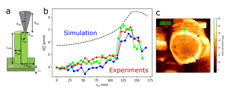
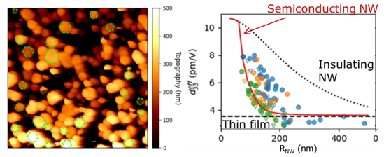
Piezoelectric and semiconducting zinc oxide (ZnO) nanowires (NWs) are excellent candidates for the fabrication of energy harvesters, mechanical sensors, piezotronic and piezophototronic devices [1]. Understanding the interplay between piezoelectricity and semiconductor physics is fundamental to enhancing the performance of these devices. Within PULSE-COM we explored the piezoelectric performance of vertically grown ZnO NWs based on Finite Element simulations in the PFM (Piezoresponse Force Microscopy) configuration. In this AFM (Atomic Force Microscope) mode, the AFM tip is placed in contact with the top surface of the NW while applying a voltage, thus inducing a deformation of the structure by the reverse piezoelectric effect [2]. These simulations included in particular the semiconducting properties of the NWs (i.e. doping concentration and surface traps) allowing the explanation of recent experimental findings under PFM: (i) The non-homogenous distribution of the piezoelectric response at the top surface of the NWs [3] (Figure 1) and (ii) the increase of the piezoelectric performance as the NW radius decreases [4]. These important findings will help us in the future to obtain guidelines for the optimization of these structures towards applications like electromechanical transducers including sensors and energy harvesters.

Figure 1: (a) Schematics of the 3D numerical simulation of the deformation of a single NW by PFM, (b) theoretical and experimental values of as a function of the location of the AFM tip at the surface of the NW, (c) experimental PFM amplitude distribution.

Figure 2: (left) AFM topography of different single ZnO NWs showing the variation in radius, (b) theoretical and experimental values of as a function of the NWs radius.
References
[1] R. Tao, G. Ardila, R. Hinchet, A. Michard, L. Montès, and M. Mouis, “Will composite nanomaterials replace piezoelectric thin films for energy transduction applications?”, in Future Trends in Microelectronics: Journey into the Unknown; Wiley, John & Sons, Inc. (2016). DOI: 10.1002/9781119069225.ch3-4.
[2] A. J. L. Garcia, T. Jalabert, M. Pusty, V. Defoor, X. Mescot, M. Montanino et al. (2022). “Size and semiconducting effects on the piezoelectric performances of ZnO nanowires grown onto gravure-printed seed layers on flexible substrates”. Nanoenergy Advances, 2(2), 197-209.
[3] T. Jalabert, M. Pustya, A. J. Lopez Garcia, A. Cresti, M. Mouis, G Ardila, “ZnO nanowires based piezoelectric transducers: the role of size and semiconducting properties”, Proceeding of SPIE (2023). (Proceedings Volume 12584, Smart Materials for Opto-Electronic Applications; 1258406 (2023) https://doi.org/10.1117/12.2665500)
[4] T. Jalabert, M. Pusty, M. Mouis, G. Ardila, (2023). “Investigation of the diameter-dependent piezoelectric response of semiconducting ZnO nanowires by Piezoresponse Force Microscopy and FEM simulations” Nanotechnology, 34(11), 115402.


