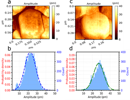
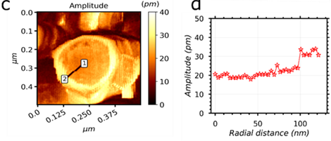
Piezoelectric and semiconducting zinc oxide (ZnO) nanowires (NWs) are excellent candidates for the fabrication of energy harvesters, mechanical sensors, piezotronic and piezophototronic devices [1]. Understanding the interplay between piezoelectricity and semiconductor physics is fundamental to enhancing the performance of these devices. In PULSE-COM, within a strong collaboration of ENEA and UGA partners [2], a new strategy to improve the measurements and analysis at the nanoscale have been developed. The stragegy is based on piezoresponse force microscopy (PFM) and was applied to study the piezoelectric performances of ZnO NWs vertically grown on seed layers deposited by gravure printing [3] onto flexible substrates (Figure 1). We demonstrated the influence of the NW radius (Figure 2): a NW with smaller diameter (100 nm) led to a higher piezo response PFM amplitude (25 pm) when compared to a wider NW (200 nm wide with a PFM amplitude response of 20 pm). We also demonstrated that the piezoresponse was not homogeneous at the surface of the NW (Figure 3), this effect could only be explained by considering the semiconducting properties (such as free carriers) and not only the piezoelectric properties of the material. These important findings will help us in the future to obtain guidelines for the optimization of these structures towards applications like electromechanical transducers including sensors and energy harvesters.

Figure 1 – (a) SEM images of ZnO NWs grown on sintered ZnO seed layer on ITO/PET flexible substrate, (b) Topography (c) PFM amplitude and (d) phase distributions on ZnO grown PET-ITO after 1 h annealing of the seed layer deposited by gravure printing.

Figure 2 – Piezoelectric PFM amplitude maps and histograms of the top of individual ZnO NWs with an approximatively radius of (a) 200 nm and (b) 100 nm.

Figure 3 – (a) Piezoelectric amplitude distribution measured by PFM on a single ZnO NW (b), along with the radial distance between points 1 and 2.
[1] R. Tao, G. Ardila, R. Hinchet, A. Michard, L. Montès, and M. Mouis, “Will composite nanomaterials replace piezoelectric thin films for energy transduction applications?”, in Future Trends in Microelectronics: Journey into the Unknown; Wiley, John & Sons, Inc. (2016). DOI: 10.1002/9781119069225.ch3-4.
[2] Garcia, A. J. L., Jalabert, T., Pusty, M., Defoor, V., Mescot, X., Montanino, M., … & Ardila, G. (2022). Size and Semiconducting Effects on the Piezoelectric Performances of ZnO Nanowires Grown onto Gravure-Printed Seed Layers on Flexible Substrates. Nanoenergy Advances, 2(2), 197-209.
[3] G. Sico, M. Montanino, C. T. Prontera, A. D. G. Del Mauro, C. Minarini, “Gravure printing for thin film ceramics manufacturing from nanoparticles”. Ceram. Int. 44, 19526–19534 (2018).


