Another method for improving the PMP properties is the opal-inverse opal imprinting on PMP surface.
The inverse opals [1] are ordered porous solids, a sort of photonic crystals [2] much cheaper and with large number of layers. The main characteristic of photonic crystals is the existence of the photonic band gap (PBG) which makes visible light or IR strongly reflected. The existence of the PBG induce a wide range of applications such as sensors, waveguides, fiber and optical integrated circuits, and many others [3].
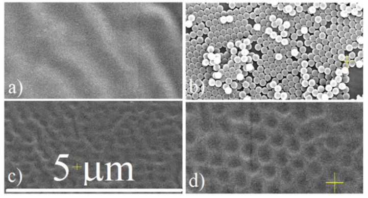
The imprinted opal/inverse opal on PMP was realized by using the “hanging drop” method using polystyrene spheres of 300 nm diameter infiltrated with sodium silicate. The obtained samples have been analysed by SEM.

SEM images of: a) PMP polymer film surface; b) PS nanosphere monolayer onto the PMP polymer film; c) circular holes produces by PS nanosphere embossing of the PMP film; d) regular array of holes onto the polymer film which can induce Bragg reflection of the light.
Conclusions
Imprinted inverse-opal pattern of hundreds of nm was realised on PMP, which can induce a PBG with potential applications in laser mirrors or sensors.
[1] E. Armstrong, C. O’Dwyer, Artificial opal photonic crystals and inverse opal structures-fundamentals and applications from optics to energy storage, J. Mater. Chem. C 3 (2015) 6109-6143.
[2] K.A. Arpin, A. Mihi, H. Johnson, A.J. Baca, J.A. Rogers, J.A. Lewis, P.V. Braun, Multidimensional Architectures for Functional Optical Devices, Adv. Mater. 22 (2010) 1084-1101.
[3] L. Carroll, J.-S. Lee, C. Scarcella, K. Gradkowski, M. Duperron, H. Lu, Y. Zhao, C. Eason, P. Morrissey, M. Rensing, S. Collins, H.Y. Hwang, P. O’Brien, Photonic Packaging: Transforming Silicon Photonic Integrated Circuits into Photonic Devices, Appl. Sci. 6 (2016) 426.


